

Why Choose K-TEK for Semiconductor Precision Parts
K-TEK combines 5-axis CNC machining, CNC milling, CNC turning, WEDM, EDM, grinding, heat treatment, surface treatment, assembly support, ISO 9001:2015 quality management, ERP-supported production control, tight-tolerance machining and fine surface finish control. These capabilities help engineering buyers reduce supplier communication cost and keep precision components aligned with approved drawings.
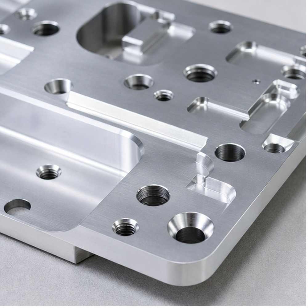
Clean Machined Surfaces
Edges, holes and pockets are processed with attention to burr control and surface consistency.
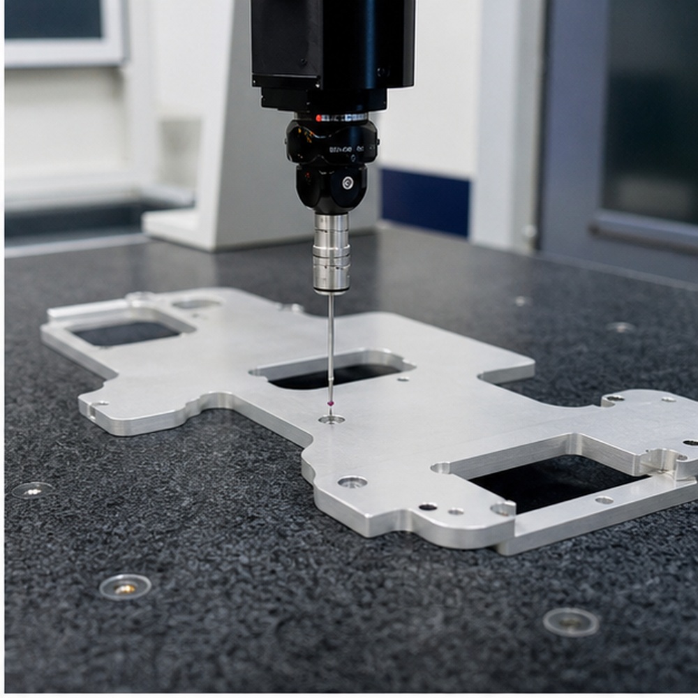
Flatness and Position Accuracy
Equipment plates, carriers and fixtures are checked for mounting accuracy and assembly stability.
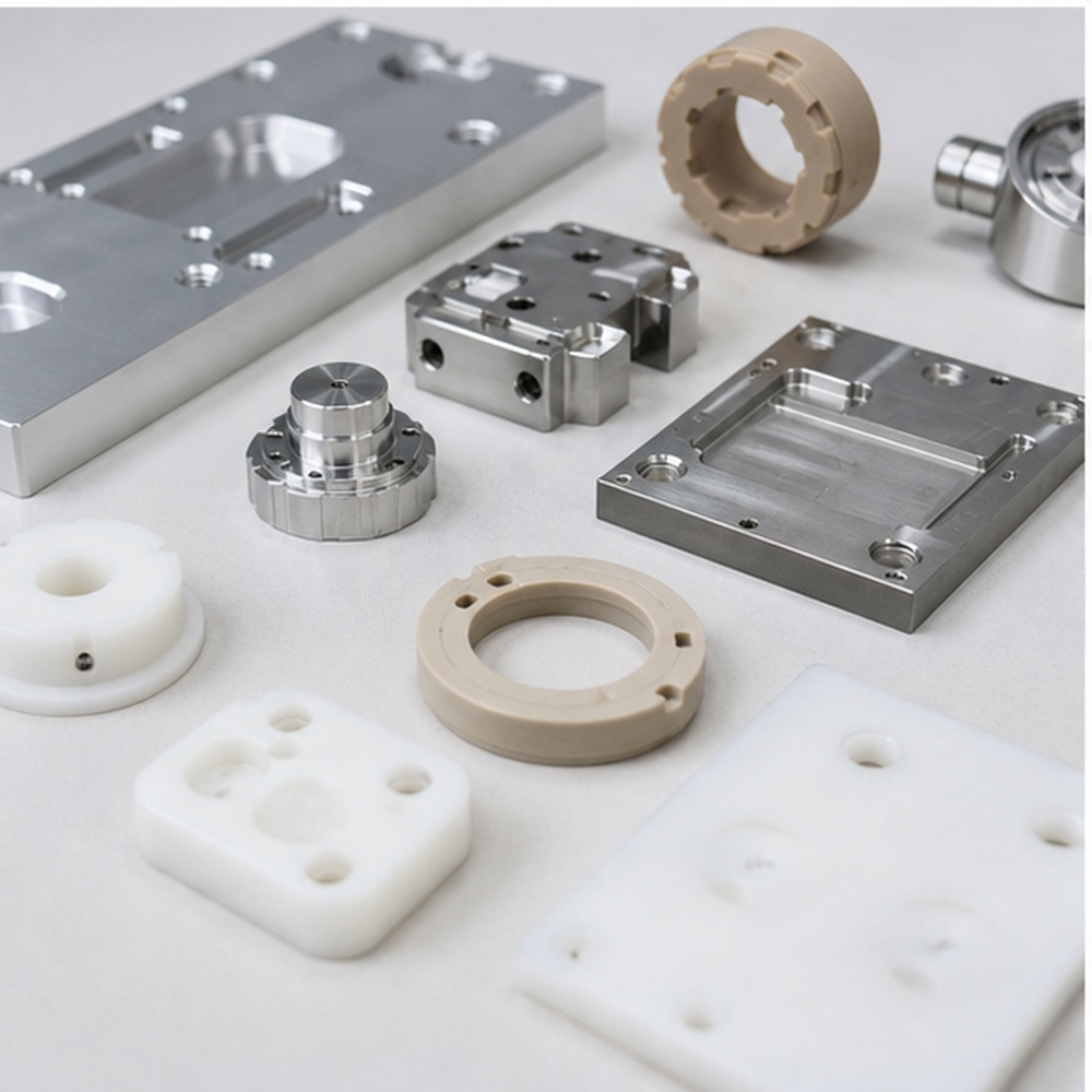
Material Stability
Aluminum, stainless steel and engineering plastics can be selected according to weight, insulation and corrosion needs.
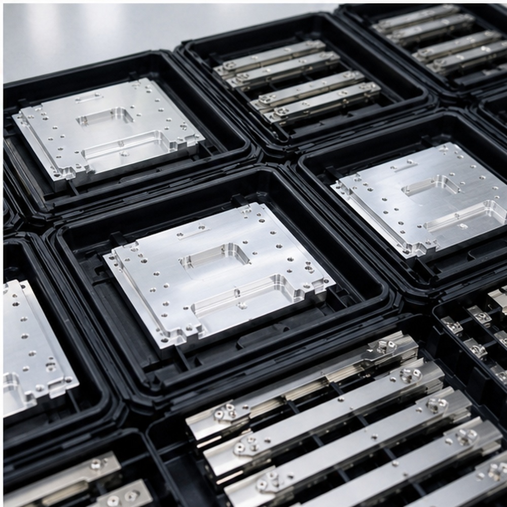
Repeatable Process Control
ERP-supported production helps maintain consistency between prototype, pilot and repeat orders.
From Semiconductor Prototype to Reliable Production
Semiconductor equipment development requires controlled prototypes before installation in machines or test systems. K-TEK can support sample machining, engineering modifications, pilot batches and repeated production while keeping inspection requirements visible for critical surfaces and mounting interfaces.
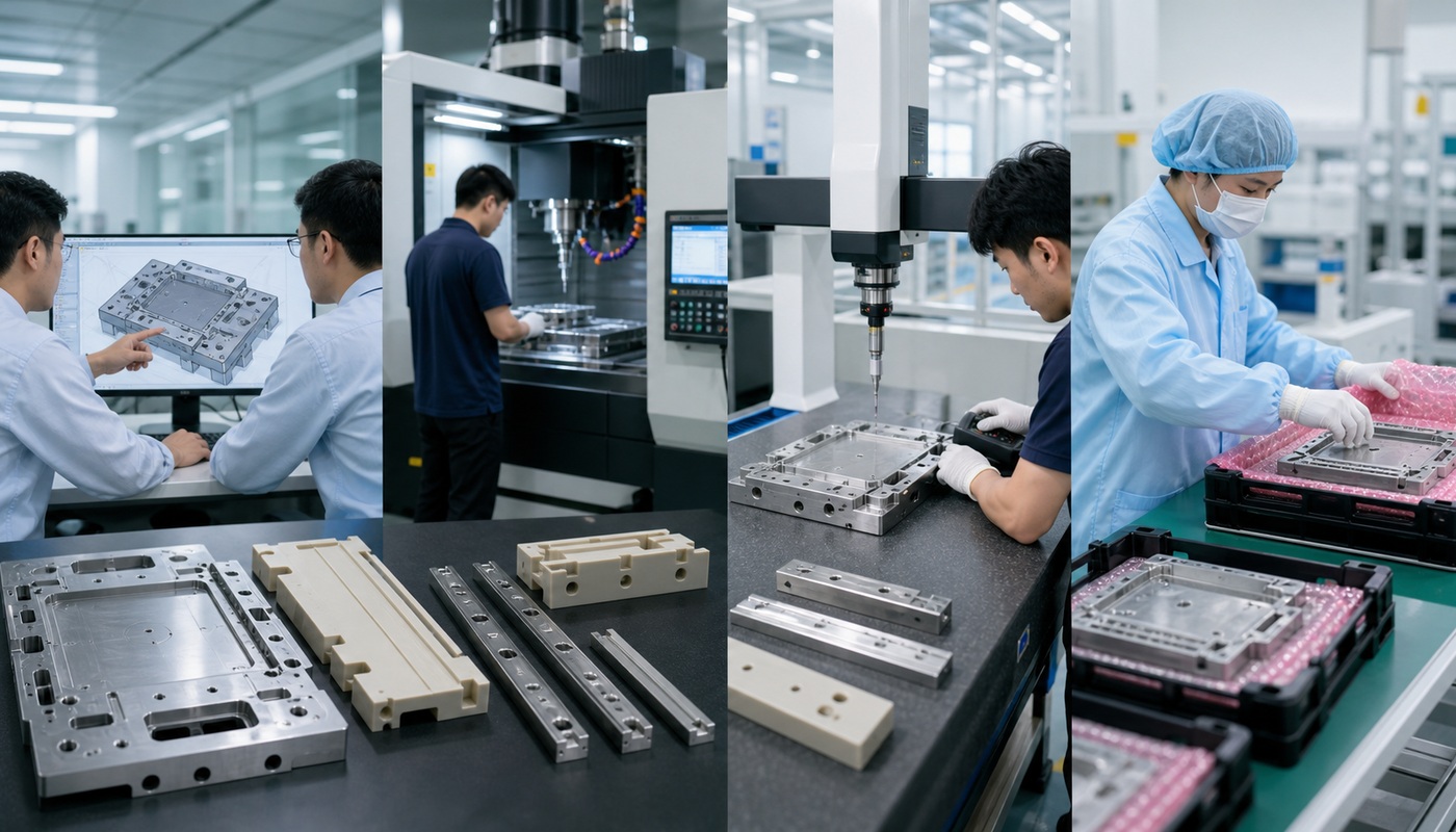
Drawing Review
Review CAD files, material notes, tolerances and finishing requirements before machining.
Prototype Machining
Produce functional samples for fit, assembly, surface and engineering validation.
Pilot Batch
Confirm process stability, inspection method and packaging before repeat production.
Repeat Production
Keep approved dimensions, finishes and inspection points consistent across batches.
Manufacturing Capabilities for Semiconductor Components
Select the right process according to part geometry, tolerance, material and production volume. K-TEK can combine CNC milling, turning, 5-axis machining, EDM, WEDM, grinding and surface treatment for complete precision part manufacturing.
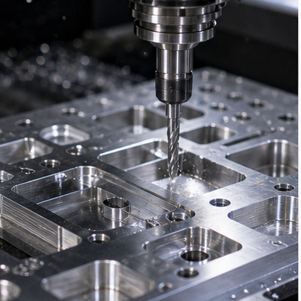
Precision CNC Milling
For plates, blocks, carriers, fixture bases and multi-pocket equipment parts.
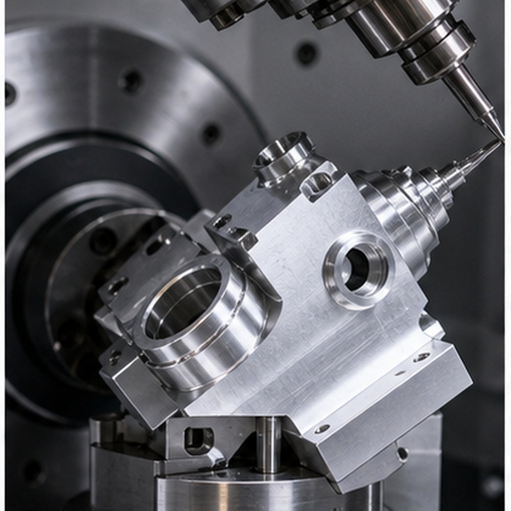
5-Axis Machining
For compact components with angled ports, multi-side features and reduced re-clamping needs.
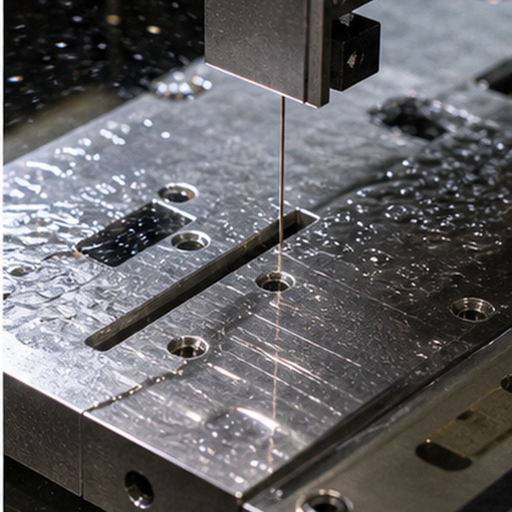
EDM / WEDM
For fine slots, internal profiles and difficult-to-machine precision features.
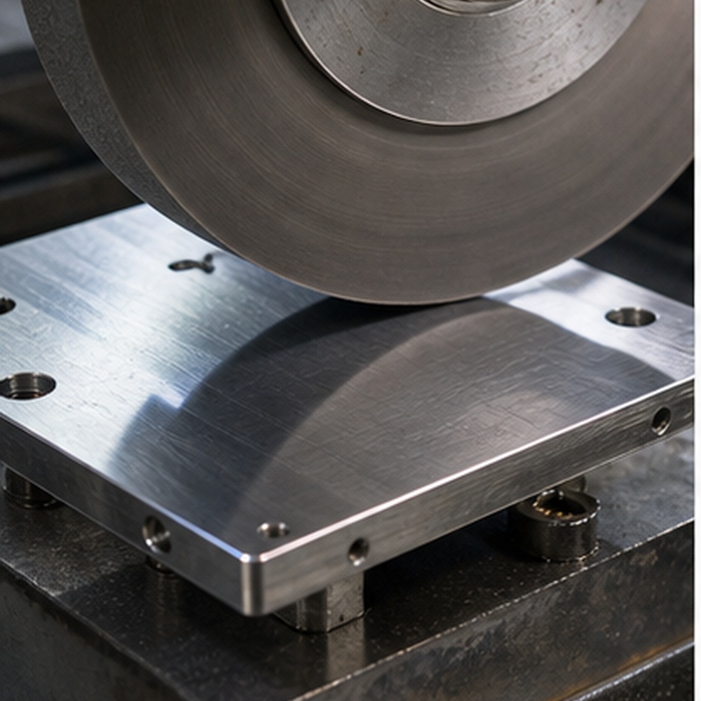
Grinding
For flat contact surfaces, controlled thickness and stable assembly datum surfaces.
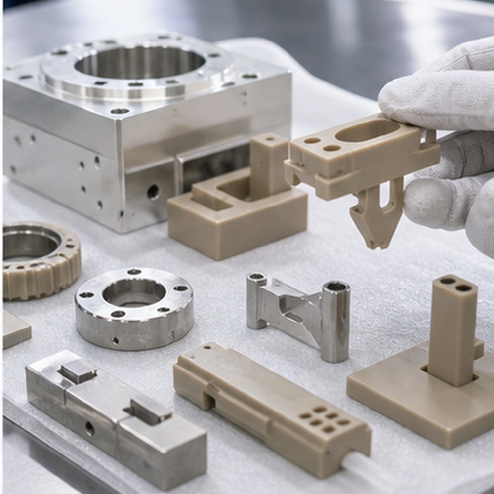
Surface Treatment
For anodizing, passivation, electropolishing or nickel plating depending on equipment conditions.
Semiconductor Parts We Manufacture
K-TEK manufactures custom semiconductor precision parts based on buyer drawings, 3D files and functional requirements. The section should help Google and AI search understand the exact component scope instead of using generic industry wording.
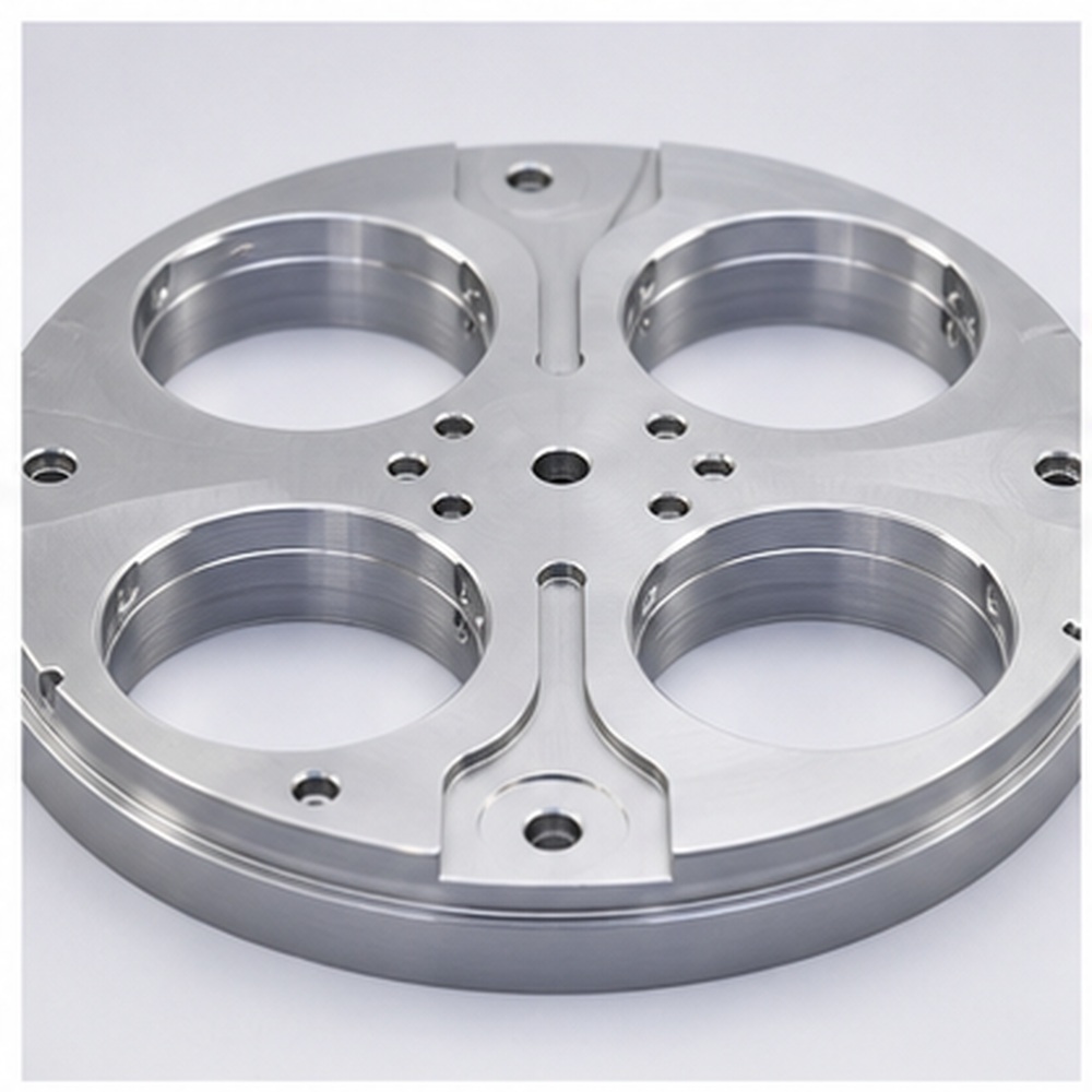
Wafer handling fixtures
Custom machined wafer handling fixtures manufactured according to drawing, material, tolerance and finish requirements.
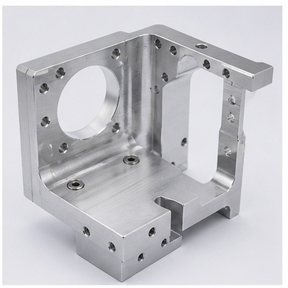
Inspection equipment brackets
Custom machined inspection equipment brackets manufactured according to drawing, material, tolerance and finish requirements.
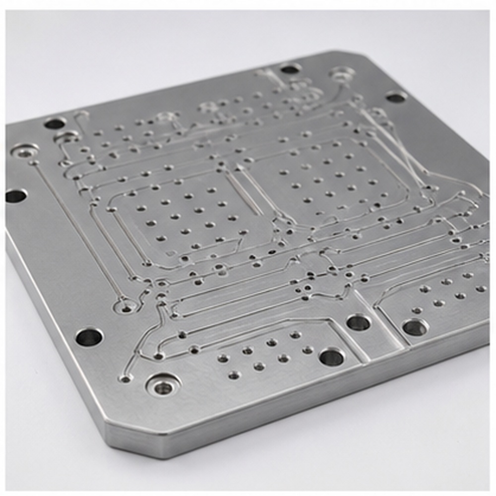
Vacuum fixture plates
Custom machined vacuum fixture plates manufactured according to drawing, material, tolerance and finish requirements.
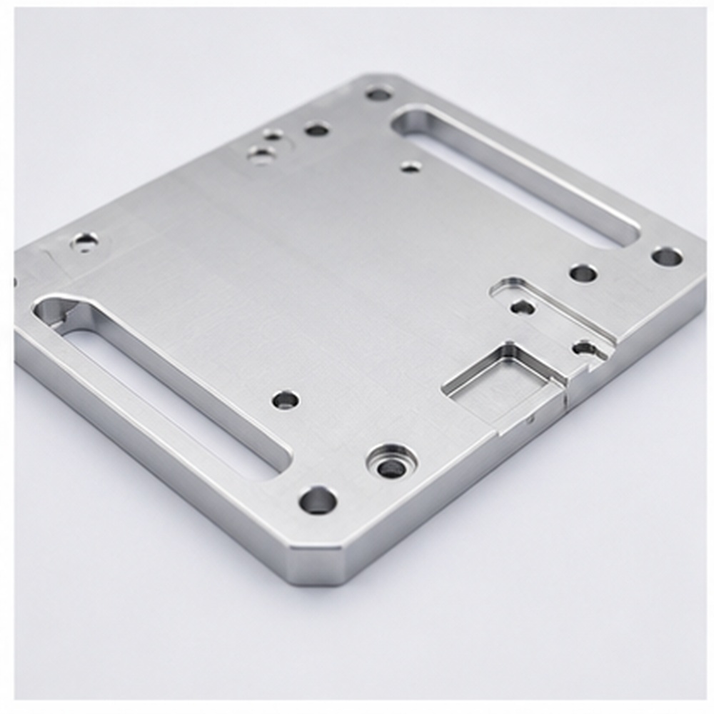
Precision aluminum carriers
Custom machined precision aluminum carriers manufactured according to drawing, material, tolerance and finish requirements.
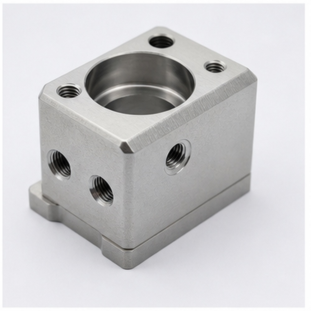
Sensor mounting blocks
Custom machined sensor mounting blocks manufactured according to drawing, material, tolerance and finish requirements.
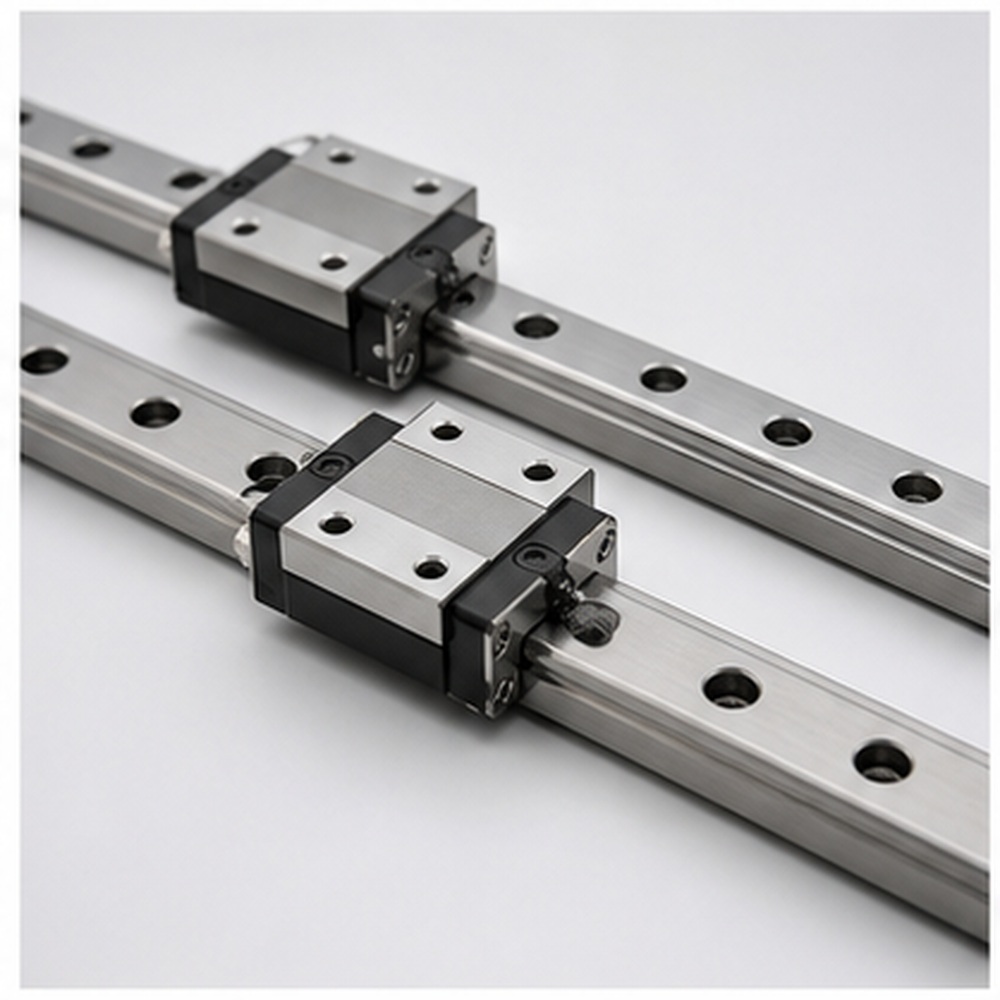
Stainless steel guide parts
Custom machined stainless steel guide parts manufactured according to drawing, material, tolerance and finish requirements.
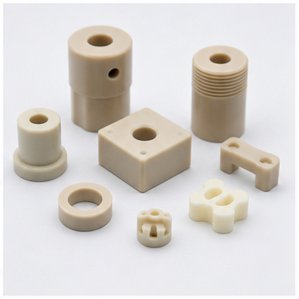
Engineering plastic insulators
Custom machined engineering plastic insulators manufactured according to drawing, material, tolerance and finish requirements.
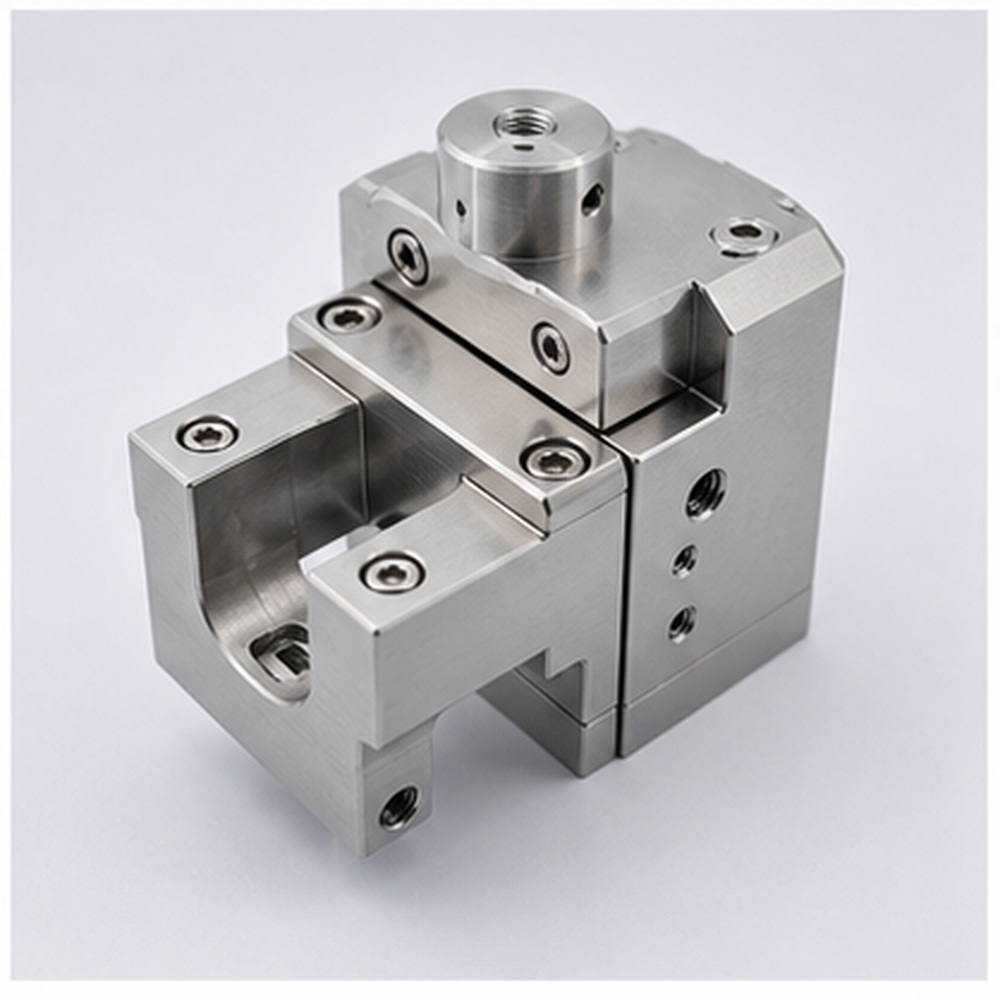
Automation tooling components
Custom machined automation tooling components manufactured according to drawing, material, tolerance and finish requirements.
Materials for Semiconductor Machined Parts
Material selection affects weight, strength, corrosion resistance, conductivity, surface finish and long-term assembly stability. The table below helps buyers compare common material choices for semiconductor precision components.
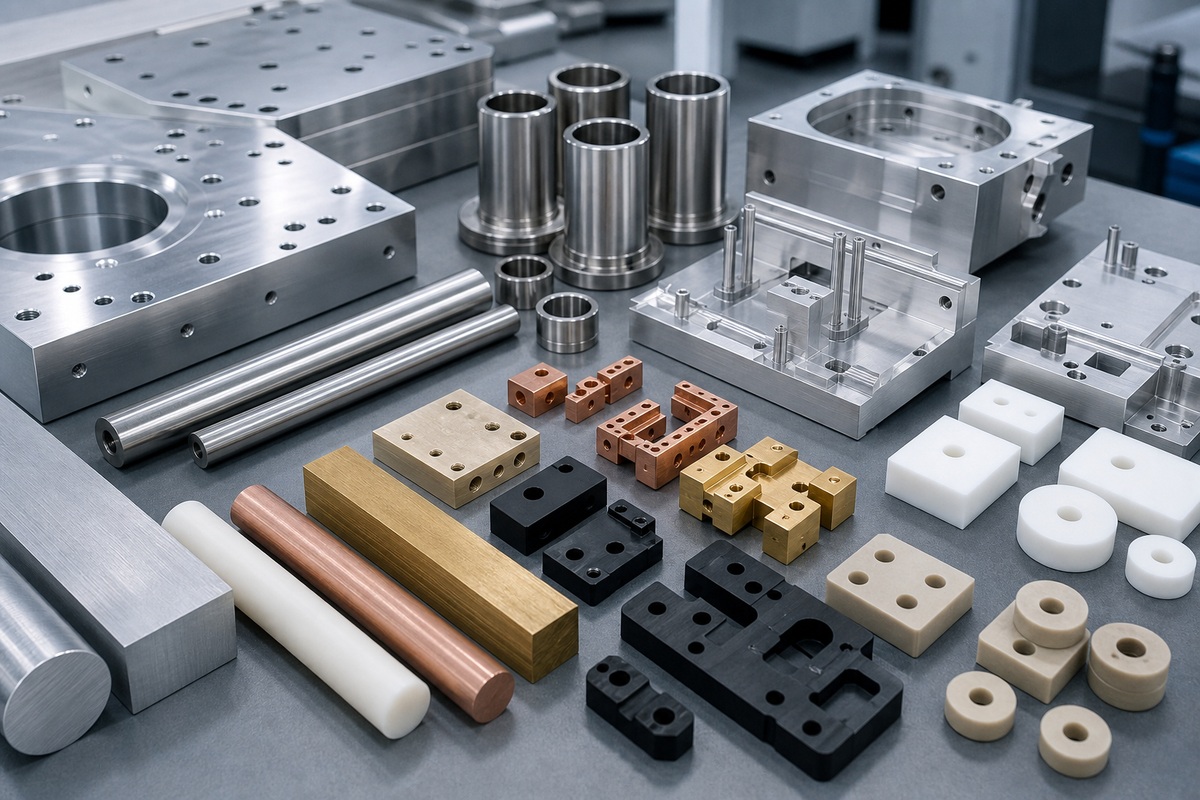
| Material | Best For | Notes |
|---|---|---|
| Aluminum 6061 / 7075 | Lightweight plates, carriers and equipment frames | Confirm final grade, heat treatment and finish according to drawing and application environment. |
| Stainless Steel 304 / 316 | Corrosion-resistant fixtures, guides and hardware | Confirm final grade, heat treatment and finish according to drawing and application environment. |
| PEEK / POM / PTFE | Insulation, low-friction and chemical-resistance applications | Confirm final grade, heat treatment and finish according to drawing and application environment. |
| Copper / Brass | Conductive parts, grounding blocks and thermal components | Confirm final grade, heat treatment and finish according to drawing and application environment. |
Surface Finishing Options for Semiconductor Components
Surface finishing should be selected according to material, assembly environment, appearance requirements and functional performance. K-TEK can coordinate machining and post-processing so finished parts meet both dimensional and visual expectations.
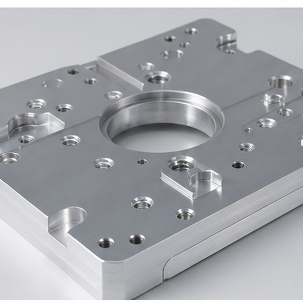
Clear or hard anodizing for aluminum
Use clear or hard anodizing for aluminum when the project requires matching protection, appearance or functional performance for semiconductor parts.
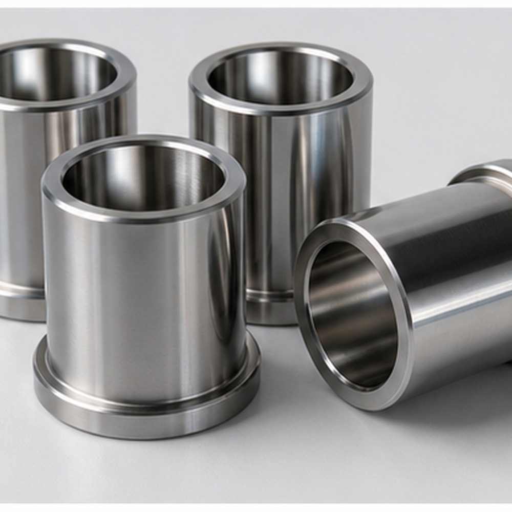
Electropolishing for stainless steel
Use electropolishing for stainless steel when the project requires matching protection, appearance or functional performance for semiconductor parts.
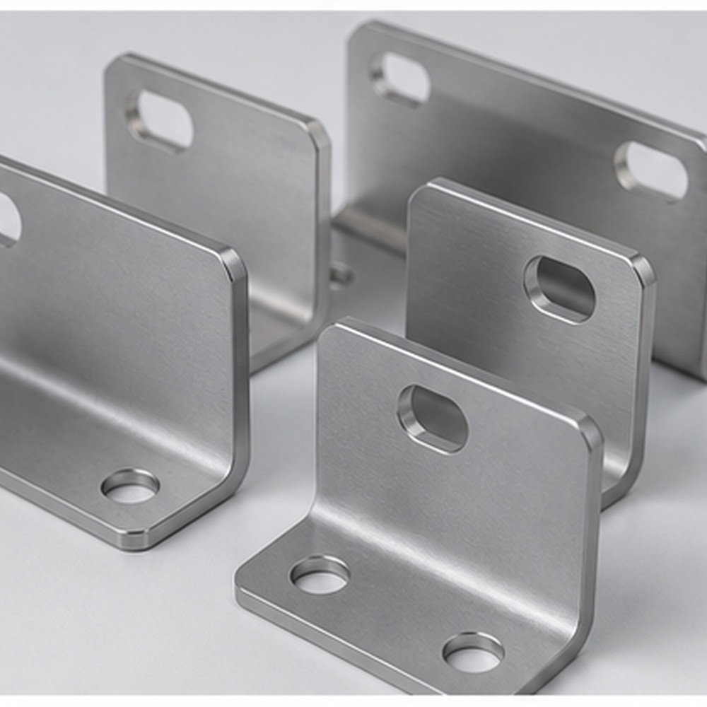
Passivation for corrosion resistance
Use passivation for corrosion resistance when the project requires matching protection, appearance or functional performance for semiconductor parts.
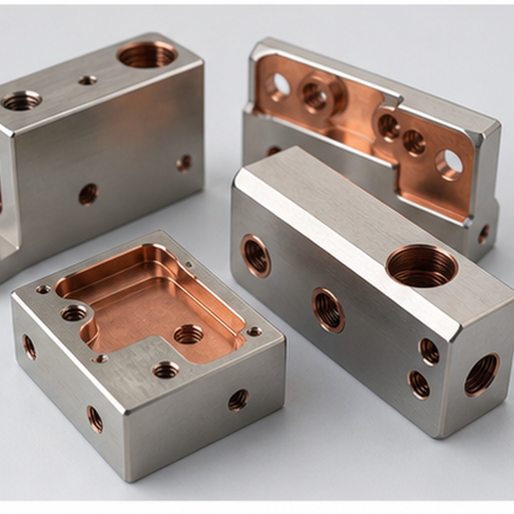
Nickel plating for equipment hardware
Use nickel plating for equipment hardware when the project requires matching protection, appearance or functional performance for semiconductor parts.
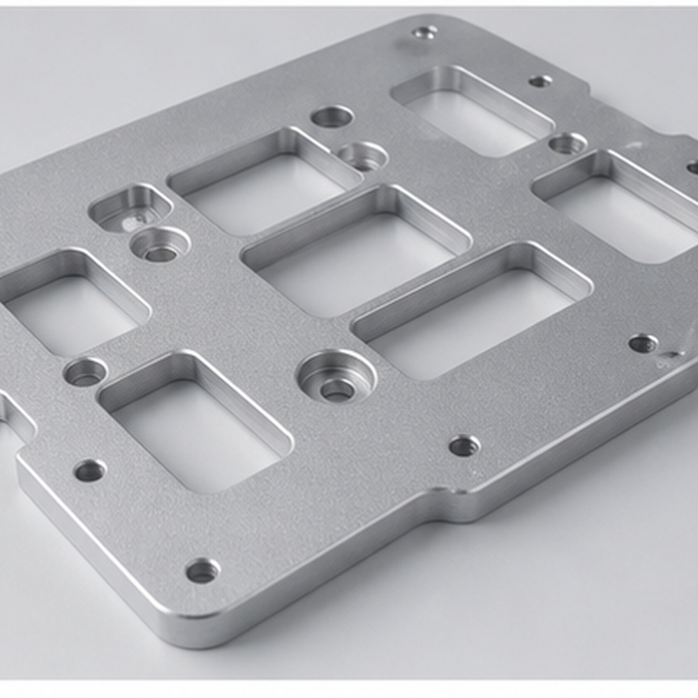
Fine bead blasting for uniform matte surface
Use fine bead blasting for uniform matte surface when the project requires matching protection, appearance or functional performance for semiconductor parts.
Quality Assurance for Semiconductor Precision Parts
Quality control should focus on the dimensions and surfaces that affect final assembly. K-TEK checks critical tolerances, hole positions, surface condition and finish quality before parts are packed for delivery.
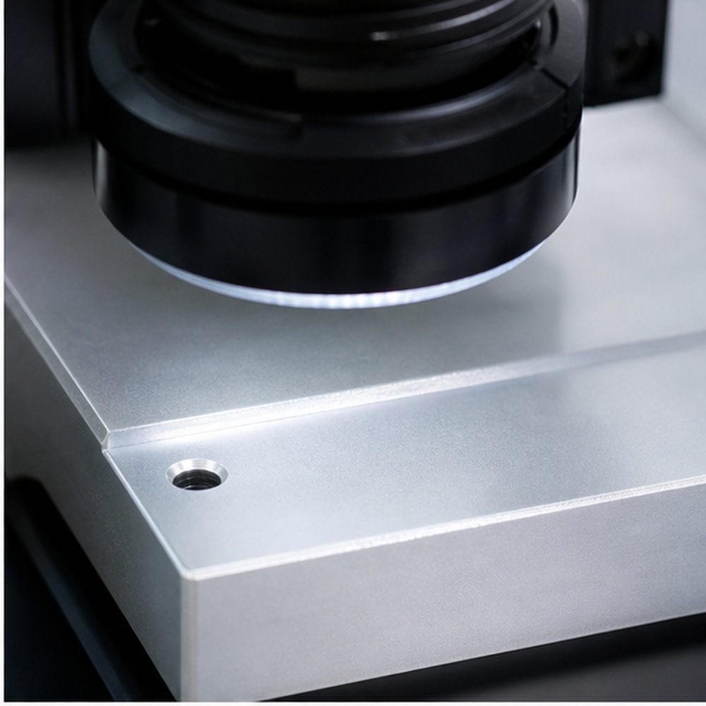
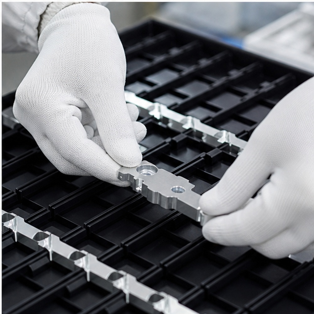
Burr and edge inspection
Burr and edge inspection is controlled according to drawing requirements and project-specific inspection points.
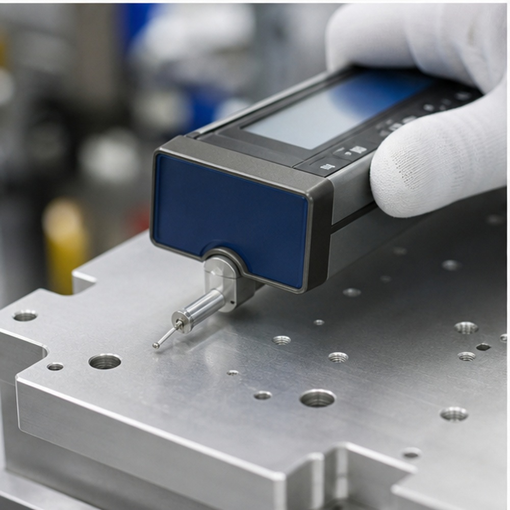
Flatness and parallelism measurement
Flatness and parallelism measurement is controlled according to drawing requirements and project-specific inspection points.
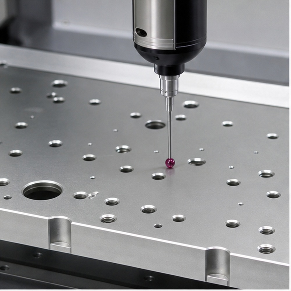
Thread and hole position verification
Thread and hole position verification is controlled according to drawing requirements and project-specific inspection points.
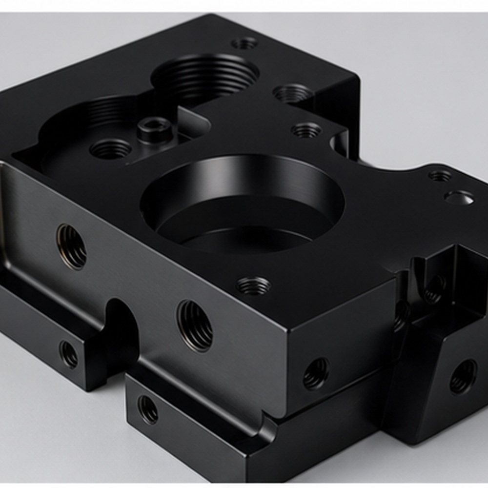
Surface roughness check for contact areas
Surface roughness check for contact areas is controlled according to drawing requirements and project-specific inspection points.
Critical dimension report for equipment assembly
Critical dimension report for equipment assembly is controlled according to drawing requirements and project-specific inspection points.
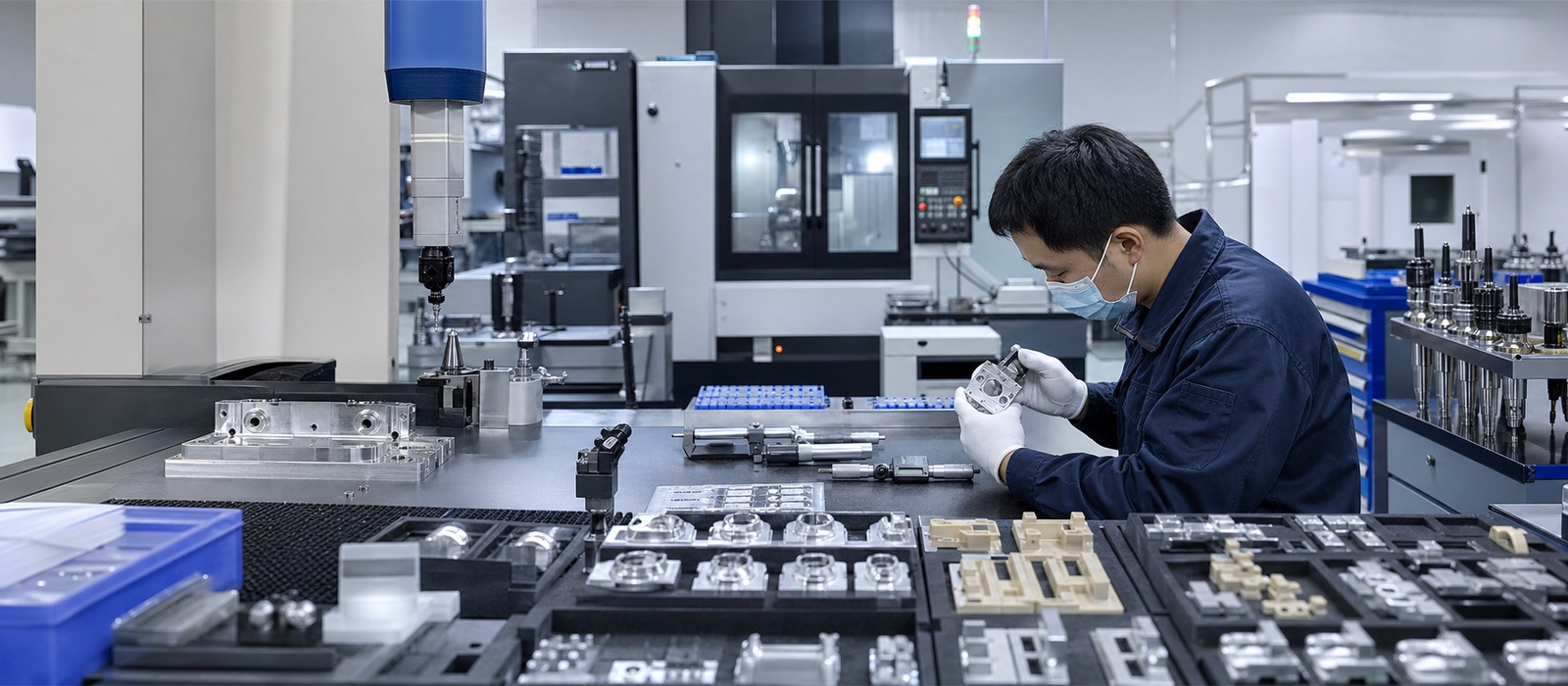
Factory Strength for Semiconductor Parts Manufacturing
Use real photos of precision machined plates, clean fixture components, inspection tables and CMM measurement. Avoid semiconductor chip stock imagery unless used only as background. K-TEK should present factory capability through real machining, inspection, material staging and finished part images rather than generic stock visuals.
Semiconductor Manufacturing Case Studies
Use case cards to show the machining process, material, finish and inspection value behind real semiconductor components. Case studies should be concise but specific enough to support SEO and GEO answer extraction.
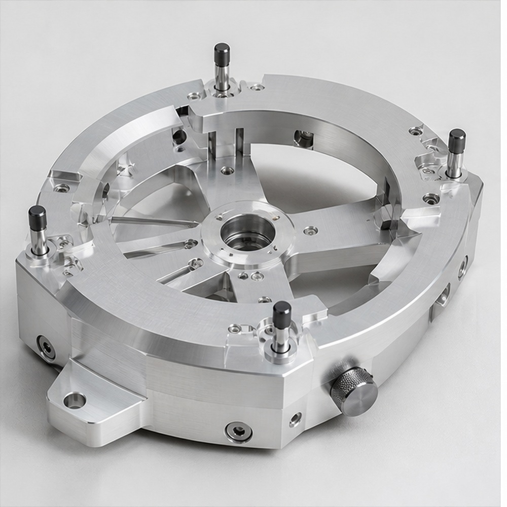
Wafer Fixture Plate
Precision milled aluminum fixture plate with pocket consistency, flatness inspection and hard anodized surface.
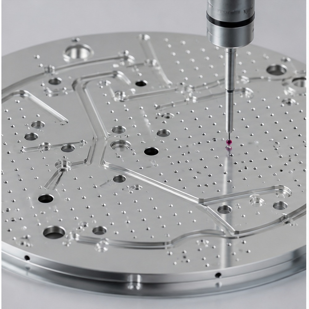
Vacuum Equipment Bracket
Stainless steel bracket machined with controlled sealing-related surfaces and passivation after inspection.
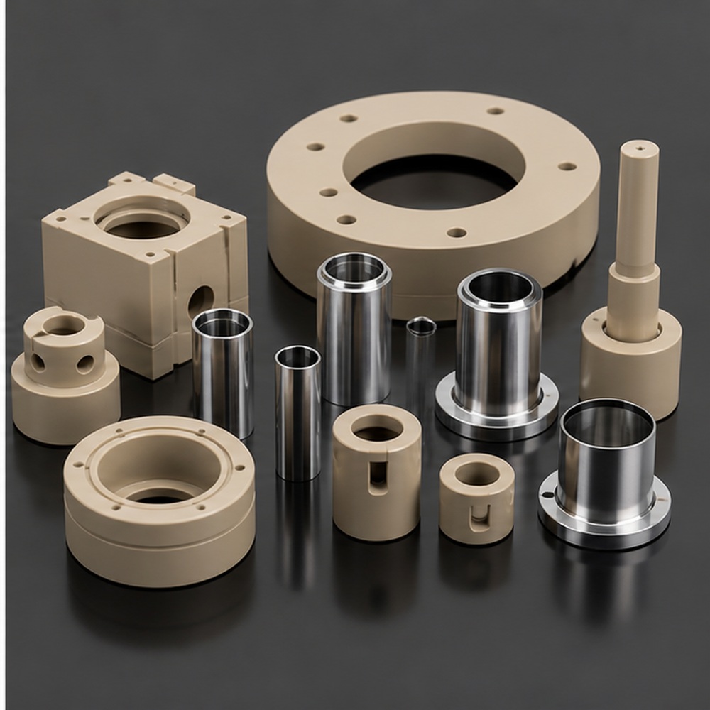
PEEK Insulating Guide
Engineering plastic guide part machined for clean edges, stable slots and repeatable assembly fit.
FAQs About Semiconductor Precision Machining
FAQ should answer real buyer questions about materials, tolerances, prototype support, inspection and surface finishing. Use visible accordion content and add FAQPage structured data.
Can K-TEK machine semiconductor equipment parts?
Yes. We can machine plates, fixtures, carriers, brackets, guide parts and custom equipment components for semiconductor-related systems.
How do you control burrs on precision equipment parts?
Burr-sensitive edges are reviewed during programming, machining, deburring and final inspection according to part requirements.
Can you machine engineering plastics for semiconductor equipment?
Yes. PEEK, POM, PTFE and other engineering plastics can be used for insulating, low-friction or chemical-resistant components.
Can you support pilot batches before repeat production?
Yes. We can support prototypes, pilot batches and repeated orders after sample approval.


